Table of Contents
- Introduction
- Overview
- Theory of Operation
- Circuit Design
- Summary
- Table of Figures
- Table of Equations
Introduction
Pulse Width Modulation (PWM) is a form of digital signal encoding where a unipolar, rectangular waveform’s duty cycle is varied to control the average voltage delivered to a load. The signal is characterized by a fixed frequency and amplitude, with the effective average voltage determined by the ratio of the pulse width to the total time period. This ratio is often referred to as the “duty factor”, or “duty cycle”. In other words a 75% duty cycle (0.75) means the signal is on for 75% of the time period, and off for the remainder 25%.
In this article the design of an analog circuit to generate a voltage-controlled PWM waveform is discussed, analyzed, and designed.
Overview
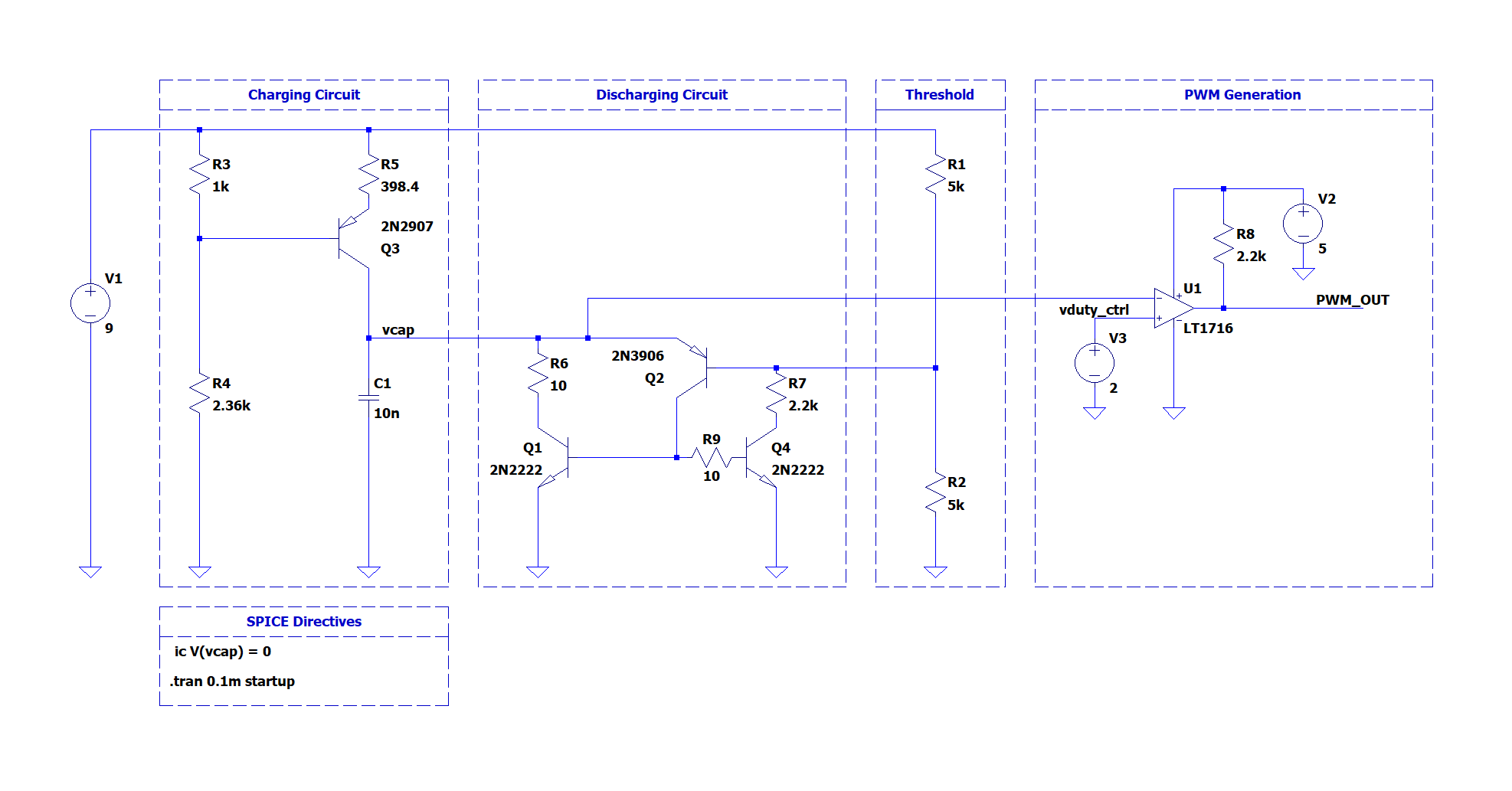
This proposed circuit is one of many that are capable of producing a pulse-width modulated (PWM) waveform. PWM is used everywhere from car headlights to display backlights due to the electrical efficiency of the waveform and ease of use with external devices (e.g. avoiding high resistance areas in transistor switches). This circuit consists of a constant current source that charges a capacitor in a linear fashion, a threshold driven discharge circuit which resets the signal, and a comparator which compares a set voltage point to the resultant sawtooth waveform thereby generating the ultimate pulse width modulated waveform.
Theory of Operation

In this circuit, $Q_3$ serves as a constant current source when it is in the forward-active region of operation. The voltage divider $R_3$, and $R_4$ set the base bias voltage and the operation point in conjunction with $R_5$. Capacitor $C_1$ serves as a charge storage element producing a linearly increasing voltage with a slope that is proportional to the charging current.
As the capacitor charges, its voltage increases linearly, limited by the voltage source, until it exceeds the threshold set by the threshold voltage divider $R_1$, and $R_2$. When this voltage on the capacitor exceeds $V_{th}+0.7V$, $Q_2$ begins conducting. This triggers $Q_4$ through positive feedback, rapidly discharging the capacitor to ground. The transistors $Q_2$ and $Q_4$ form a current mirror that pulls the discharge node below approximately $1V$. This SCR-like latch remains on until current drops ensuring that the transistors completely turns off. Without $Q_1$, at higher currents the latch may remain partially on, preventing proper reset.
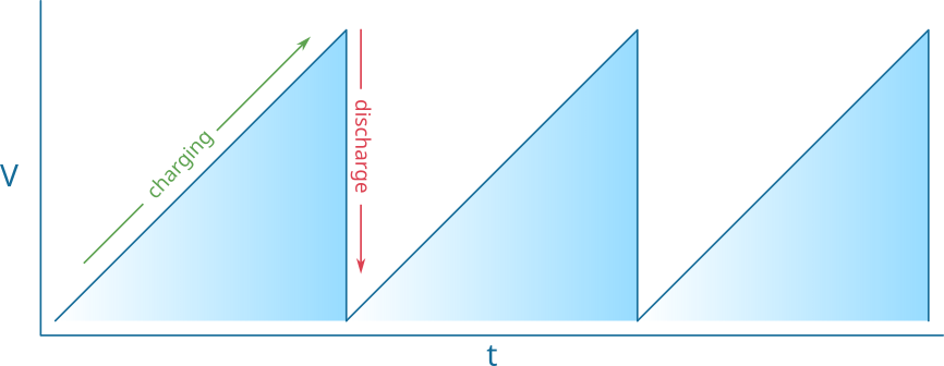
The charge-discharge waveform is a linear ramp, followed by a sharp discharge, ultimately forming a sawtooth waveform. This signal is then compared against a DC voltage in the comparator $U_1$. As the sawtooth waveform exceeds the setpoint the output of the comparator resets to $0V$. When the sawtooth waveform is less than the setpoint the output is $5V$, set by $V_2$. This comparator output is now a fixed frequency but variable duty cycle waveform, also known as pulse width modulated, since the width of the pulse can be varied, or modulated.
This circuit is broken down into three key blocks. The charging circuit which is responsible for charging the capacitor, the discharge circuit which enabled the astable oscillating behavior, and the comparator which generates the final PWM output.
Circuit Design
To realize this circuit the design requirements must be established. The following are based on a common 100kHz, 5V output but can be tailored to suit a specific application and recalculated.
| Parameter | Value |
|---|---|
| Target Frequency | 100kHz |
| Capacitance | 10nF |
| Output Signal | 5V |
| Supply Voltage | 9V |
Constant Current Charging Circuit
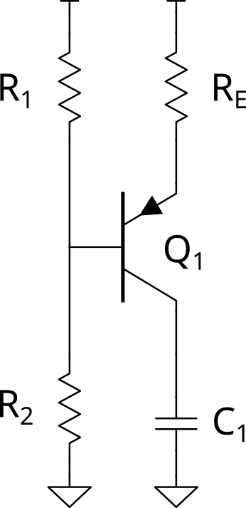
The charging block consists of three resistors, one PNP transistor, and a capacitor. This forms a constant current source which is responsible for charging a capacitor. When a current source is connected to a capacitor a linear ramp voltage output is produced.
Charging Mode
When a voltage is applied to a capacitor in an R-C network the voltage rise is not linear but exponential. This means that the slope is constantly changing. This leads to reduced spatial resolution in our PWM signal. We can exploit a property of capacitors where we apply a constant current instead of a constant voltage and by doing so a constant voltage slope can be generated. This removes the nonlinearity from the system but adds additional drive requirements for control.
To design this circuit, first determine the desired operational frequency, select a capacitor, then calculate the required charging current. A constant current source can then be realized in combination with the system operating voltage source.
Charging Current
\[\Large I = C \frac{dV}{dt}\]To output a 100kHz sawtooth means that a transition must occur from $V_L$ to $V_H$ in $\frac{1}{100e3} = 10 \mu s$. The current required to charge the capacitor within this time is as follows:
\[\Large t_{sec} = \frac{C (V_f - V_i)}{I}\]Derivation
This equation is derived from the integration of the differential.
First, rearrange the equation to isolate $dV$.
\[\Large dV = \frac{I\cdot dt}{C}\]Next, integrate $dV$.
\[\Large \int_{V_i}^{V_f} = V_{f} - V_{i}\]Finally, integrate $dt$.
\[\Large \int_0^t \frac{I}{C} dt= \frac{I}{C} \int_0^t dt = \frac{I\cdot t}{C}\]Rearrange to isolate time.
\[\Large t_{charge} = \frac{C (V_{f} - V_{i})}{I}\]Performing a dimensional analysis verifies equation units:
\[\Large Farads \cdot \frac{Volts}{Seconds} = Amps\]Approximations
Note that these equations are a close approximation. They do not account for the fall time, or nonidealities of the components such as parasitic effects, DC bias, etc.
Transistor Circuit Design
| Parameter | Reference | Value | Units |
|---|---|---|---|
| Transistor | - | 2N2907 | - |
| Transistor Beta | $\beta$ | $250$ | - |
| Supply Voltage | $V_s$ | $9$ | $V$ |
| Saturation Current | $I_s$ | $10\mathrm{e}{-15}$ | $A$ |
With the current determined to be $5mA$, the constant current source can be designed. Starting with the base current which is calculated by dividing the collector current by the common-emitter gain factor also known as Beta ($\beta$).
\[\Large i_b = \frac{i_c}{\beta} = \frac{5mA}{250} = 20\mu A\]Beta Variation
Transistor Beta ($\beta$) will vary from transistor to transistor and should be accounted for in critical applications. This analysis assumes ideal components.
The emitter operation point is selected to be $7V$, or $2V$ above our capacitor charging output voltage target. This is done to ensure that the transistor remains in the forward active region to produce a constant current output. That is, the emitter should remain at $7V$ when driving the full $5mA$.
Insufficient Voltage Consequence
The consequence of not operating in the forward active region is a loss of constant current output. If the transistor is no longer forward biased such as in the case of insufficient voltage headroom, it will transition to the saturation region as the capacitor charges. This results in acting as a resistor producing a nonlinear output instead of the desired linear ramp.
The emitter resistor can be determined using Ohms law. This calculation is taking the desired voltage drop across the resistor and dividing it by the total current to obtain the resistor required to achieve this effect.
\[\Large R_E = \frac{V_S - V_{op}}{i_b + i_E} = \frac{9V - 7V}{20\mathrm{e}{-6}A + 5\mathrm{e}{-3}A} = \frac{2V}{5.02\mathrm{e}{-3}A} = 398.4 \Omega\]Before the voltage bias point can be determined $V_{EB}$ must be calculated. This factor is commonly omitted where a $V_{BE}$ of $0.7V$ is assumed. Since the saturation current is known the total error of the calculations can be minimized by calculating this factor.
\[\Large V_{BE} = V_T \ln\frac{i_b}{I_s / \beta} = 25mV \cdot\ln\frac{20\mu A}{10\mathrm{e}{-15} / 250} = 673.4mV\]Now, the voltage bias point can be determined.
\[\Large V_{EB} = V_{s} - (i_E \cdot R_{E}) = 9V - 2V -0.6734V = 6.327V\]Based upon these values the voltage divider can now be calculated.
\[\Large \frac{R_2}{R_1 + R_2} \cdot V_s + \left ( \frac{1}{R_1} + \frac{1}{R_2} \right )^{-1} \cdot i_b = V_{EB}\]This expression is stating that the voltage divider output plus the offset voltage caused by the base calculated as the divider in parallel should be equal to the target Emitter-Base voltage.
Rearranging for $R_2$ results in the following compact expression:
\[\Large R_2 = \frac{V_{EB}\cdot R_1}{V_s - V_{EB} + i_b \cdot R_1}\]This method accounts for the error caused by the base current. $R_1$ would be chosen to be the closest preferred resistor value, and then $R_2$ calculated based on the above formula.
$\Large R_1 = 1000\Omega$
\[\Large R_2 = \frac{6.327V \cdot 1000\Omega}{9V - 6.327V + 20\mu A \cdot 398.4\Omega} = 2.36k\Omega\]These values can now be simulated.
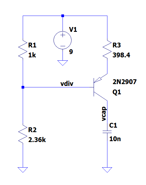
LTSPICE DC Analysis Output:
| Parameter | Value | Units |
|---|---|---|
| V(vdiv): | 6.33477 | V |
| V(n002): | 7.03152 | V |
| V(n001): | 9 | V |
| Ic(Q1): | -0.00492198 | A |
| Ib(Q1): | -1.8988e-05 | A |
| Ie(Q1): | 0.00494097 | A |
| I(R3): | 0.00494097 | A |
| I(R1): | 0.00266523 | A |
| I(R2): | 0.00268422 | A |
| I(V1): | -0.00760621 | A |
This results in a constant current source of 4.921mA, corresponding to an error of only -1.58%.
\[\Large \frac{4.921mA - 5mA}{5mA} \cdot 100\% = -1.58\%\]This provides a close approximation but does not account for component manufacturing tolerances. When transitioning to a manufacturable device trimming resistors would be necessary to achieve tighter tolerances, however, other designs using operational amplifiers may be more desirable for precision applications.
Discharge
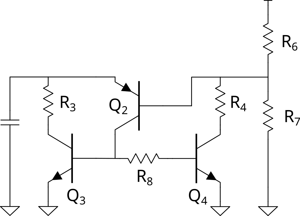
The discharge circuit consists of one PNP transistor, and two NPN transistors. The PNP-NPN pair has matched transistor gains and forms an SCR. It functions by triggering at a set voltage level. When the voltage at the emitter goes above the threshold voltage by $V_{BE}$ the transistor begins conducting. This current is amplified again by Q4 which increases the current gain. As this occurs the NPN from the capacitor to ground turn on and allow even more current for a faster turn off.
Notably, without this second NPN transistor the voltage will be limited by the $V_{BE}$ junction of the PNP transistor in addition to the $V_{CE}$. This comes out to approximately $1V$. This functions when the current source is only charging microamps, but when we want to charge the capacitor at faster rates with higher current these transistors form essentially a linear regulator in that they do not turn off. This prevents the system from oscillating as expected.
The values for $R_4$ and $R_3$ were set to be $2.2k\Omega$ and $10\Omega$ to limit the maximum current through the device. The 2N2222 has a $600mA$ maximum continuous current rating therefore at $10\Omega$ and a $5V$ maximum charge we limit it to $5/10 = 0.5A$. The addition of resistor $R_8$ can be added to increase the gain of $Q_3$ to avoid a Darlington pair or higher gain transistor. A value of $10\Omega$ was chosen for the simulation example.
The threshold is set by the discharge voltage divider and begins conducting when the PNP transistor is in the saturation region.
\[\Large V_{th} = \left( \frac{R_7}{R_6 + R_7} \cdot V_s \right) + 0.7V\]Comparator
The comparator generates the pulse-width modulation output. In this arrangement the duty factor control voltage is connected to the non-inverting input, while the the ramp signal is applied to the inverting pin.
If the duty factor control voltage is set to 2.5V then the output will be “high” until the ramp exceeds $2.5V \pm V_{os}$. If the ramp has a maximum voltage of 5V, then this will produce a 50% ON PWM signal. The frequency of the ramp will dictate how fast the PWM transitions between OFF and ON.
\[\Large DF = \frac{V_{ctrl}}{V_{max}} = \frac{2.5}{5} = 0.5\]In this arrangement the larger the voltage applied, the higher the duty cycle up to 100%. This logic could be inverted by reversing the input terminals. That is, feed the control voltage source setpoint into the inverting input. In that case an increase in voltage would cause a decrease in duty factor.
Many comparators feature an open drain output. This requires the addition of a resistor from the supply to the output of the comparator. The value of $2.2k \Omega$ was chosen arbitrarily, however, once the output device is known this value could be tuned to minimize the quiescent current drawn.
The voltage source could be created with a potentiometer connected between the supply and ground with the wiper connected to the input terminal of the comparator.
Comparator Alternative
Comparators are designed for faster operation than an operational amplifier. Op-Amps have a longer recovery time when driven to saturation and are intended to be used with feedback. While an Op-Amp could be used for this application, comparators are purpose built for this application and are therefore recommended.
Summary
In this article, an analog circuit for generating a voltage-controlled pulse-width modulated (PWM) waveform was presented. The circuit was divided into three functional blocks: the charging circuit, the discharge circuit, and the comparator. Using standard circuit analysis methods, design equations were derived to approximate circuit behavior, enabling tolerance evaluation and refinement through simulation.
Accurate operation depends on ensuring that transistor stages maintain sufficient voltage headroom to remain in the forward-active region. This approach demonstrates that PWM waveforms can be implemented using fundamental analog components while maintaining predictable and controllable performance.
Table of Figures
- PWM Circuit Schematic
- Charge-Discharge Waveform
- Constant-Current Charging Circuit
- LTSPICE Simulation Schematic
- Discharge Circuit Schematic
- Discharge Simulation Waveform
- Discharge Simulation Waveform, Transition View
- PWM Simulation Waveform
Table of Equations
- Capacitor - Charging Current
- Capacitor - Constant Current Charge Time
- Capacitor Charging Current
- Charging Units Dimensional Analysis
- Transistor Base Current
- Emitter Resistor Calculation
- Base-Emitter Voltage Drop Calculation
- Emitter-Base Operating Point Calculation
- Voltage Divider Calculation
- Concise Voltage Divider Formula
- Voltage Divider, R2 Calculation
- Constant Current Error Calculation
- Discharge Threshold Approximation
- Duty Factor Equation