Table of Contents
- Introduction
- Pi Attenuator
- Implementation Tips
- Monte Carlo Simulation
- Summary
- Project Files Download
- Appendix A: Formulas
- Table of Figures
- Table of Equations
Introduction
Attenuators are a fundamental building block in RF and microwave system design. Their primary function is to reduce signal power by a precise amount while presenting a matched impedance to both source and load to ensure that reflections and standing waves are minimized throughout the system. Because attenuators are passive, bilateral networks, they attenuate power in both the forward and reverse directions. Unequal impedance configurations require a separate design methodology and are outside the scope of this article.
This article covers the design, component selection, and power rating of a Pi-topology resistive attenuator network. Further, a Monte Carlo method for validating manufacturing tolerances is also presented.
Equations
All equations assume equal source and load impedances. ($Z_s = Z_L = Z_o$). Designs requiring differing impedances are not covered in this article.
Pi Attenuator

One of the more frequently used attenuator types is the PI attenuator. It is called “Pi” because it resembles the $\Large \pi$ symbol. It consists of one series and two shunt resistor elements.
The design equations are straightforward; however, the power dissipation analysis warrants careful attention due to the asymmetric power dissipation in the network, discussed subsequently in detail.
\[\Large \textcolor{BurntOrange}{R_{shunt}} = \textcolor{WildStrawberry}{Z_\emptyset} \left( \frac{10^{\frac{\textcolor{Cerulean}{A_{dB}}}{20}}+1}{10^{\frac{\textcolor{Cerulean}{A_{dB}}}{20}}-1}\right)\]Example Calculation
Now that the basic formula is known, an attenuator can be realized. In practice a $10dB$ attenuator is a common value to have, which is the basis of the article. A $10dB$ attenuator would take a 5-Watt source signal and attenuate it to 0.5-Watts (one-half Watt) at the load. This is ideal for protecting the input stage of an RF Amplifier for example.
| Parameter | Value | Units |
|---|---|---|
| System Impedance | 50 | $\Large \Omega$ |
| Input Power | 36.99 | dBm |
| Input Power | 5.00 | W |
| Attenuation | 10 | dB |
Calculate Ideal Shunt Element
To calculate the ideal resistor values simply replace the input impedance $Z_\emptyset$ with the system impedance, in this case $50 \Omega$. Then, substitute the $A_{dB}$ (attenuator factor) with the desired attenuation value.
\[\Large \textcolor{BurntOrange}{R_{shunt}} = \textcolor{WildStrawberry}{Z_\emptyset} \left( \frac{10^{\frac{\textcolor{Cerulean}{A_{dB}}}{20}}+1}{10^{\frac{\textcolor{Cerulean}{A_{dB}}}{20}}-1}\right) \rightarrow \textcolor{WildStrawberry}{50} \left( \frac{10^{\frac{\textcolor{Cerulean}{10}}{20}}+1}{10^{\frac{\textcolor{Cerulean}{10}}{20}}-1}\right) = \textcolor{BurntOrange}{96.25 \Omega}\]The equations then result in the ideal resistance values. In reality, however, resistors are usually only offered in specific values, called the E-series values, and are subject to manufacturer variation, called tolerance. Typical values are $5\%$, $1\%$, and $0.5\%$ but custom resistors can be purchased and attenuators are also offered as monolithic devices.
Tolerance Impact
Remember that a change in resistance not only changes its power dissipation, but also the system impedance and the ultimate system attenuation. Ensure that your tolerance is within acceptable margins before mass production.
Power Dissipation
Since the power dissipation in this attenuator is asymmetric careful attention is warranted as well as consideration of the derating factors due to the input resistor seeing the full source voltage whereas the load sees only the attenuated voltage.
The attenuator power dissipation is calculated using standard linear network analysis methods following Ohm’s law starting with conversion from Power to RMS Voltage to generate the starting values. The RMS voltage represents the equivalent DC value that delivers the same average power to a resistive load.
Signal Source Assumption
The RMS voltage calculation assumes a sinusoidal waveform with a crest factor of $\sqrt2 \approx 1.414$. Other waveforms require a different crest factor to be applied. Ensure that the correct factor is applied when the signal is non-sinusoidal otherwise your calculations will have an additional source of error.
Power to Voltage Calculation
Following Ohm’s law the RMS voltage can be calculated if the power and the resistance are known. Note that this is the RMS voltage and not the peak voltage that would be used to determine the maximum voltage of the attenuator.
\[\Large V_{RMS} = \sqrt{P \cdot R}\]Worked Voltage Example
For a 5-Watt source in a $50 \Omega$ system the voltage would be as follows:
\[\Large \sqrt{5W \cdot 50 \Omega} = 15.811V\]Note that a dimensional analysis can be used to confirm the units are correct.
\[\Large \sqrt{W \cdot \Omega} = \sqrt{V^2} = V\]Calculate Branch Current
With the source voltage known, branch current are determined by successive application of Ohm’s law and the current divider rule. Refer to the circuit schematic for component designations.
\[\Large I_{R_1} = \frac{V}{R_1}\]The remainder branch current can be calculated.
\[\Large I_{R_2} = \frac{V_{R_1}}{\left ( R_2 + \left[ R_3 \parallel R_L \right] \right)}\]Next, apply the current divider equation to determine how the current is split between the load resistance and $R_3$.
\[\Large I_{R_3} = I_{R_2} \cdot \frac{R_L}{R_3 + R_L}\]Finally, to calculate the current through the load the following equation can be used.
\[\Large I_{R_L} = I_{R_2} \cdot \frac{R_3}{R_3 + R_L}\]Calculate Dissipated Power
Once the currents are known, power dissipation for each resistor can be calculated using Ohm’s law.
\[\Large P = I^2 R\]where
- $P$ is power.
- $I$ is current.
- $R$ is resistance.
For the example $10dB$ attenuator the power dissipated in each resistor is as follows:
| Resistor | Current | Impedance | Power |
|---|---|---|---|
| $R_1$ | $0.16426 A$ | $96.25 \Omega$ | $2.597W$ |
| $R_2$ | $0.15201 A$ | $71.1 \Omega$ | $1.643W$ |
| $R_3$ | $0.0519694 A$ | $96.25 \Omega$ | $0.260W$ |
| $R_L$ | $0.100041 A$ | $50.0 \Omega$ | $0.500W$ |
| Total | - | - | $5.000W$ |
Verify with Power Balance
After calculating the power dissipation in each element ensure that a quick power balance has been performed to ensure that the sum of dissipation in the system including the load equals the input power. This closure check confirms calculations are consistent.
Implementation Tips
Trace Geometry
When implementing RF circuits, the package size matters. When trace geometry changes such as transitioning to a pad – impedance discontinuities result. These discontinuities cause impedance mismatches in the transmission line. Whenever possible, and especially important as the frequency content increases, discontinuities in the transmission line should be minimized by matching the trace width at the target impedance to the component pad width. This may require removal of the ground plane beneath the component to accommodate a wider trace. Wider traces also exhibit lower conduction losses due to the skin effect.
Passive Parasitics (Stray Inductance and Capacitance)
All passive components exhibit parasitics that alter their impedance characteristics with frequency. These parasitics vary by manufacturer and package. Always simulate using S-parameter or SPICE models provided by the manufacturer for highest accuracy, and validate all simulation results against measured data.
Derating
Apply appropriate derating factors for duty factor, voltage, and environmental conditions (temperature, humidity, altitude, conformal coating, etc). Power dissipation capability decreases significantly with increasing ambient temperature; consult the component manufacturers derating curve and apply appropriate thermal analysis to confirm margin. Use solid thermal vias without a thermal-relief spoke to the ground plane to reduce junction-to-ambient thermal resistance and improve heat extraction from the component. This is one place where PCB layout for thermal design can be critical to ensure a long component life.
Preferred Resistance Values
Not all resistor combinations are available off the shelf. In many cases resistor values must be combined in series or parallel to achieve the target value, or the calculated value must be rounded to the nearest available E-series value. Consider the impact of this rounding on attenuation accuracy and re-evaluate the power calculations after value adjustment.
Monte Carlo Simulation
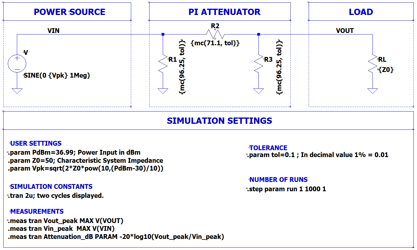
Once attenuator values are selected, manufacturing tolerance analysis is required to confirm that the design will meet specifications across production variation. Two analysis methods are commonly used:
Extreme Value Analysis (EVA) assumes all component values simultaneously reach their worst case tolerance limits. This is conservative and appropriate when:
- Production volumes are low and parts will be screened.
- Worst case performance must be guaranteed by analysis (e.g. safety-critical applications).
- The component tolerance distribution is unknown.
Monte Carlo simulation is a preferred method for volume production where component tolerances are known to follow a Uniform distribution. It provides a statistical yield prediction that guides cost-effective component grade selection.
Statistical Methods
Note that statistical methods are not an ultimate guarantee. They simply describe the probability. It is still possible to produce products that are out of specification if the Monte Carlo values are used.
What it Does
Each run in a Monte Carlo simulation assigns a new resistor value which is sampled independently from a Uniform distribution centered on its nominal value, with the deviation corresponding to the specified tolerance. This uniform assumption should be verified against the component manufacturer’s Statistical Process Control (SPC) data. Components with a gaussian or bimodal distribution will produce different results - and potentially produce non-conservative results.
Each iteration then recalculates the attenuation in response to the newly sampled component values, and logs the measurements for subsequent analysis.
Running the Simulation
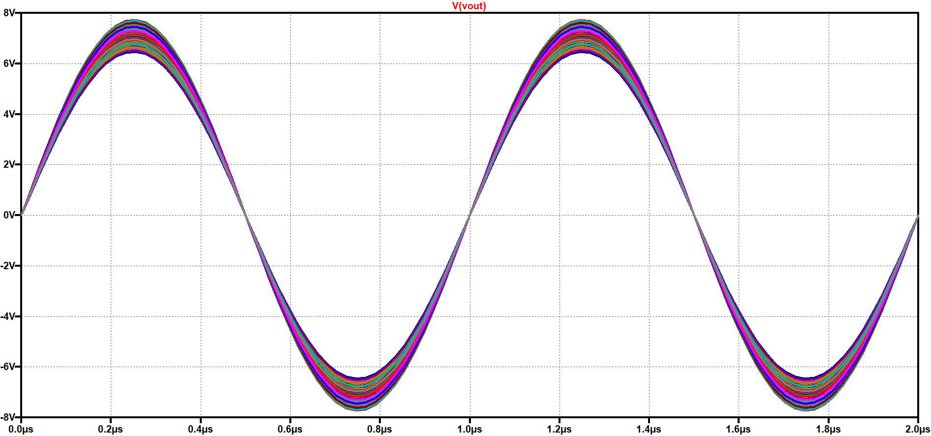
When ready, start the simulation by pressing the green button in LTSpice. Once complete, open the output log file to obtain the full dataset for analysis.
Simulation Runtime
1000 runs required approximately 30 seconds of processing time, which will vary by computer capabilities. Scale accordingly for larger run counts.
Analyzing the Results
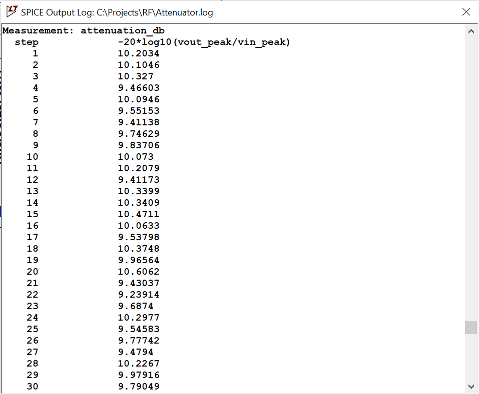
Transfer the output log data to a spreadsheet application for statistical analysis. In this simulation a $\pm 10\%$ component tolerance yields an attenuator variance of approximately $\pm 7.78\%$. This result has direct implications on system link budget allocations. For example, if the attenuation specification has a $\pm 1dB$ window, the designer must evaluate whether the $\pm7.78 \%$ variance ($\pm 0.78 dB$ at $10dB$) fits within that budget with adequate margin - and select a tighter component tolerance grade (e.g. $1\%$) if it does not.
| Parameter | Value | Units |
|---|---|---|
| Minimum Attenuation | 9.22 | dB |
| Maximum Attenuation | 10.77 | dB |
| Nominal Attenuation | 10.00 | dB |
| Variance High | 7.78% | - |
| Variance Low | -7.74% | - |
Tolerance Variation
Component tolerance variation changes not only the insertion loss but also the attenuator input and output impedance. Impedance deviation drives return loss (VSWR) degradation, which may be as critical a specification as attenuation accuracy in sensitive RF chains. The Monte Carlo dataset should therefore be analyzed for both attenuation and impedance variation.


Summary
The Pi attenuator is a deceptively simple circuit - three resistors and a well-chosen topology - yet it embodies several principles central to rigorous RF system design. Correct calculation of the shunt and series elements ensures the desired attenuation while maintaining system impedance, and the asymmetric power distribution across those elements demands careful thermal analysis before a design is ready for production.
The worked $10 dB$ example illustrates that input-side power handling governs component selection: the input shunt resistor dissipates more than five times the power of its output-side counterpart. A thermal derating strategy - accounting for ambient temperature, substrate thermal resistance, and real-world duty factor - is not optional in any design operating near rated power.
Nominal design is only the beginning. Manufacturing tolerance variation is certain, and the Monte Carlo simulation demonstrates that a $\pm 10\%$ component spread produces a non-trivial attenuation variance - a result that would directly threaten the link budget in a precision measurement or communications system. Where EVA provides a hard bound for worst-case-guaranteed designs, Monte Carlo provides the statistical yield insight that drives cost-effective component grade selection at volume.
Finally, the practical implementation considerations in this article - trace geometry, parasitic awareness, derating, and preferred value selection - are the difference between a circuit that works in simulation and one that performs reliably across production, temperature, and time. RF design is often not forgiving. Getting the fundamentals right, from the first design equation to the last thermal via, is what separates a finished product from a prototype.
Project Files Download
Project files including the Excel spreadsheet as well as the Monte Carlo demonstration can be downloaded below. LTSpice 24.0.12 was used to generate the simulation files.

Appendix A: Formulas
Voltage Divider
\[\Large V_o = V_i \cdot \frac{R_2}{R_1 + R_2}\]Current Divider
\[\Large I_x = \frac{R_{tot}}{R_x + R_{tot}} \cdot I_{tot}\]Parallel Resistance
\[\Large R_{parallel} = \frac{1}{\frac{1}{R_1} + \frac{1}{R_2} +[...] \frac{1}{R_n}}\]dBm to Watts Conversion
\[\Large P_{watts} = 10^{\frac{P_{dBm}}{10}}\div 1000\]Table of Figures
- Pi Attenuator Schematic Representation
- LTSpice Simulation Schematic
- LTSpice Monte Carlo Simulation Output Waveform
- LTSpice Output Log
- Monte Carlo Attenuation vs Run Plot
- Monte Carlo Attenuation Histogram
Table of Equations
- Attenuator Shunt Resistor
- Attenuator Series Resistor
- 10dB Attenuator Shunt Resistor
- 10dB Attenuator Series Resistor
- Ohm’s Law Power to VRMS Voltage
- Current through R1 (input shunt)
- Current through R2 (series element)
- Current through R3 (output shunt, current divider)
- Current through RL (load)
- Ohm’s Law Power Equation
- Voltage Divider
- Current Divider
- Parallel Resistance
- dBm to Watts