Table of Contents
- Introduction
- Isolation
- Isolation Types
- Signal Types
- Design
- Other Applications
- Terms
- References
- Table of Figures
- Table of Equations
Introduction
Controllers frequently interface with analog signals for both reading and commanding parts of a system. Isolation of these signals may be desirable to protect the controller, the equipment, or decrease undesirable electrical effects (noise, ground loops, over voltage, etc). Isolating digital signals tends to be straightforward, buy a digital isolator IC, add protection circuitry, supply power, choose a connector, and manufacture a board. Analog signals however can be more complicated. You can’t simply connect a DC signal through a transformer. The signals also need to be precise and accurate to minimize error.
In this article the design of a linear optical analog signal isolator for a 4-20mA current loop (which is heavily used in the process industry) is discussed.
Isolation

Isolation is the implementation of a mechanism to prevent the flow of electrical current from one part of a system to another. This is done to prevent ground loops, conducted noise, as well as prevent damage to a controller or subsystem in the event of a fault occurring. Faults could come from a number of sources including but not limited to: damaged components such as a power supply failure, incorrect wiring, and lightning strikes.
Adding an isolator to a system can increase the reliability as well as provide an easily replaceable protection mechanism to prevent damage to an expensive control system. Isolators can reduce the total system downtime as well as increase performance against noise that may exist in a system. Isolators act as barriers that can limit damage to a system similarly to how a fuse protects a power source during overcurrent events except that isolators are able to prevent fault propagation in the first place. Additionally, isolators can eliminate ground loops by breaking the electrical connection from different electrical potentials preventing the flow of current from one location to another.
Isolation Types
Isolation can come in many different forms including magnetic, optical, capacitive, and even mechanical. Within each mechanism of isolation can be a subset of architectures. When used in conjunction with additional circuitry such as an ADC, a microcontroller, and DAC each one of these can yield high performance solutions.
Transformer (Magnetic) Isolation
Transformers are frequently used to isolate power systems. They work based on transfer of magnetic fields across two (or more) coils which have a mutual inductance. Transformers alone are unable to transfer DC signals, but can be used as a tool to create galvanic isolation. In a system isolated using a transformer, signals are typically modulated, that is, converted to an AC signal. This signal is then demodulated on the secondary side to produce the original signal.
Transformers in general tend to be expensive due to their winding process, have limitations on bandwidth, but can offer bidirectional operation. Transformers are used to isolate Ethernet links, power supplies, and even industrial process signals.
Capacitive
Capacitive isolation use capacitors to isolate the field side wiring from the control side. Like transformers, capacitors cannot pass a DC signal. So the signal must again be modulated in some manner to pass the capacitive barrier and then demodulated on the control side. These systems can also be bidirectional. On the integrated circuit level silicon dioxide can act as an insulator as well as galvanic isolation barrier. Many digital isolator ICs use built in silicon dioxide barriers which form capacitors.
RF Transmitter
Radio frequency transmitters can also be considered a form of isolation, and are frequently used for sensing applications. RF links can be established over open air using an antenna, or could be transmitted over a transmission line such as coax. Galvanic isolation would only occur when signal is not electrically connected to the receiver. The addition of a capacitor to the system could provide the required isolation for a transmission line system for example.
Optical
Optical isolation uses a light source, such as an LED, and a receiver, which could be a photovoltaic module, photodiode or photoresistor for example. Optical isolation is typically uni-directional, that is, one way transfer. Bidirectional systems can be implemented with the addition of another transmit and receive circuit. These can be found in fiber optic data links for example.
In this article an optocoupler isolator will be discussed. Specifically, a linear optocoupler with servo feedback.
Signal Types
There are several different types of electrical signals that are commonly used. These are voltage and current signals. In a voltage controlled system a voltage is varied between a minimum and maximum value which corresponds to the reading intended to be transmitted. Usually the lowest value is not $0$ Volts, to allow the system to know when a fault has occurred. Instead, the minimum may be $1V$, and the maximum may be $5V$ for instance, or even $10V$ depending on the system. In a current loop system the most common is a $4-20mA$ current loop where $4mA$ represents the lowest permitted value.
Slope, offset, and conversion factors
Note that this article focuses on the implementation of the receiver isolator and therefore ignores considerations of the transducer and the signal translation. On the sensor side (transmitter) there should be mechanisms to compensations for slope, and offset which translates from engineering units to the desired analog signal range.
Voltage Loops

Voltage loops do not compensate for parasitic components within the loop. As such the transmitted signal voltage is reduced by the resistance in the line proportional to the signal current times the resistance. Additionally, they are high impedance circuits which tend to be more susceptible to noise and interference.
Current Loops

Current loops have advantages over other analog control methods, primarily because they compensate for loop resistances thereby improving accuracy. The compliance voltage is a measure of how much a loop can compensate for these loop resistances. As the resistance increases so too does the voltage drop. As long as the total loop voltage drop is less than the compliance voltage then the current loop can compensate for these drops by increasing the driving voltage to sustain the desired current.
Operational Modes

A $4-20mA$ current loop has three modes. From $0mA$ to $<4mA$ would indicate a low fault. Between $4mA$ to $20mA$ is considered normal operation. Anything above $20mA$ would be considered a high fault. Each device will have it’s own specification as to what each of these faults might indicate, however, a low fault ($0mA\ \pm$ any noise) might indicate a wiring fault.
Loop Powered Devices
While out of scope of this article there are a number of different connection types for current loops sensors. These include loop powered 2-wire systems, as well as three and four wire sensors. Of particular note is that current loop sensors can exist on only two wires which draw parasitic power from the loop. As long as these sensors stay within the minimum current draw, they can be powered by the source.
Design
The design of any electrical circuit first starts with an understanding of the goal, the system requirements, and compiling available information to understand tradeoffs.
- Reliability - The isolator should be as reliable as possible. It should not require frequent maintenance and should be easily repairable.
- Accurate - The system should accurately reproduce the input signal.
- Isolation - The device should achieve a galvanic isolation barrier. (Verify required isolation distances in layout!)
- Ease of Use - The device should be capable of being connected to a system easily and be capable of functioning as a drop in replacement for other isolators.
- Compact - The system should be compact and take up as little space as possible.
- Protection - Capable of withstanding typical handling and fault conditions.
Radiation Reliability
Photodiodes as well as LEDs tend to degrade under radiation and may not be suitable for all applications. Specific space-grade components are available that have increased reliability should be used for such applications where the system will be exposed to radiation.
Optocouplers

There are a number of optocouplers available but many optocouplers only have one emitter and one photodiode. There is instead another optocoupler also called a “Linear Optocoupler” that has one emitter, and multiple receivers. This allows for enhanced linearity and so called “Servo control”. It is called servo control because one of the photodiodes is used as feedback to control the emitter. Ideally, both photodiodes would have the same output coupling factor but under real world conditions there is some variation in the manufacturing processes. Manufacturers will then “bin” these parts by this coupling factor.
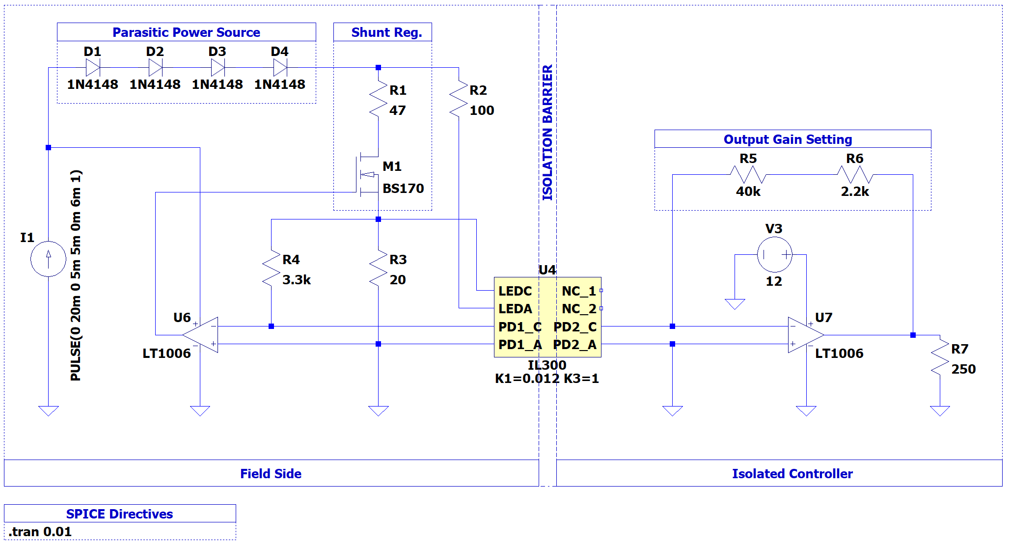
Design Overview and Operation

This circuit operates by controlling a current shunt ($Q_1$) in parallel with the emitter LED. The current shunt is controlled by the Op-Amp ($U_1$) which receives negative feedback from $R_3$ and positive feedback from $R_4$ via current from $K_1$ which is used to optimize the linearity of the signal transmission. As the LED current increases so does the voltage across $R_3$. This voltage decreases the shunt voltage while the inverse voltage across $R_4$ in series with $R_3$ generate positive feedback. There is a voltage gain due to $K_1$ being a current source. $R_4$ is chosen such that is tuned for the correct current range, and matched with the transistor $V_{gs}$ curve.
The MOSFET was chosen to be a low $V_{gs}$ on type. In this circuit a BS170 MOSFET was chosen due to it being easily available, and low cost. Other similar FETs would likely function adequately but would requiring tuning the resistors to match.
The purpose of the diode network $Dn$ is to introduce a voltage drop across the diodes sufficiently large enough to both power the Op-Amp, as well as supply enough voltage to exceed the $V_{GS}$ parameters of the selected MOSFET. These could also be replaced by an LED with sufficiently large $V_F$ and $I_{F(max)}$ if desired. This addition of diodes enables the isolator to be parasitically powered allowing it to function in a two wire current loop. While it still requires a power source on the isolated side this isolator is intended to be connected to the controller where power is usually easily available.
On the isolated side, $U_2$ generates a voltage output proportional to the current through $K_2$ multiplied by the gain setting resistor $R_5$.
Both $R_5$ as well as $R_4$ should have a potentiometer in series for manufacturing trimming for highest accuracy.
Simplified Example
The circuit provided in the simplified design overview does not include compensation networks, supply capacitances, input protection and so on. Adding these features may greatly improve the design based upon your specific application.
Design Equations
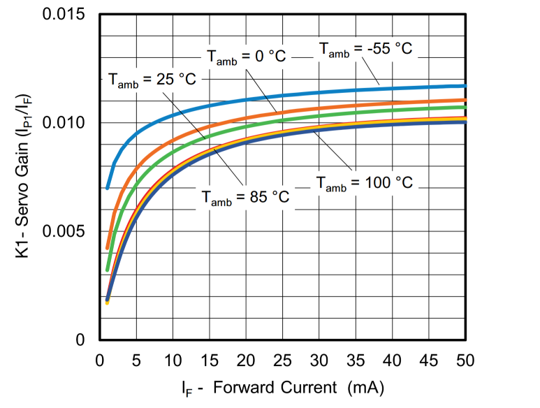
The goal of the current shunt is to keep the LED in the linear region of operation while allowing maximum dynamic range. If the LED had a linear range of operation that encompasses the entire output range of the current loop then the current shunt may not be needed. In this example $10mA$ has been chosen as the target for an input of $20mA$ due to it being a specified parameters in the IL300. Referring to the servo gain vs forward current chart will reveal that linear operation drops off quickly after this threshold.
Recall from Ohm’s law that $V=I\cdot R$. Therefore the voltage generated by the feedback photodiode should be the same as is generated by the current across the current sense resistor, $R_3$ as described by the following equation:
\[\Large I_{P1} \cdot R_4 = I_{R_3} \cdot R_{3}\]The feedback photodiode current is proportional to the LED forward current and the feedback gain coefficient, $K_1$. The feedback gain coefficient for the IL300 is specified as a minimum of $0.005$ to a maximum of $0.015$ with a typical value of $0.009$. This means that for every $1 mA$ through the LED the photodiode will produce $9\mu A$. ($K_1 = I_{P1}/I_F$). Assuming a $K_1$ factor of $0.012$ and a $R_3$ of $20 \Omega$ with a $20mA$ maximum current then $R_2$ needs to be chosen such to match this voltage.
\[\Large 120\mu A \cdot R_4 = 20mA \cdot20\Omega\] \[\Large R_4 = \frac{20mA \cdot 20\Omega}{120 \mu A} \rightarrow \frac{400mV}{120\mu A} = 3.\overline{333}k \Omega \approxeq 3.3k \Omega\]Tolerance Effects
Tolerance effects have not been ignored for these calculations. The effects of manufacturing tolerance can be compensated for using potentiometers to tune the circuit during assembly.
The current generated in the photodiodes is proportional to the current through the LED, however, $I_{P1}$ and $I_{P2}$ will have some variation. Under ideal circumstances these should both be the same currents but due to manufacturing tolerances and process variation they will differ slightly. The following equations describe the relationship between the photodiodes and the current through the LED. Note that the IL300 is binned into different transfer gains since the minimum value can be $0.56$ with a maximum of $1.65$ but this parameter is over the manufacturing lot not a specific bin. To ensure that your product has a suitable transfer gain factor you must specify the correct product part number.
| Bin | Minimum $K_3$ | Maximum $K_3$ |
|---|---|---|
| 1 | 0.557 | 1.618 |
| 2 | 0.765 | 1.181 |
| 3 | 0.851 | 1.061 |
| 4 | 0.851 | 0.955 |
| 5 | 0.945 | 1.061 |
where:
- $\Large I_{P1}$ is feedback photocurrent.
- $\Large K_1$ is feedback gain.
- $\Large P_2$ is output photocurrent.
- $\Large K_2$ is output gain.
- $\Large K_3$ is transfer gain ($K_2 / K_1$).
Bill of Materials
| Designator | Value | Note |
|---|---|---|
| Diodes | 1N4148 | Could be LED, or other diodes. |
| MOSFET | BS170 | Low $V_{gs}$ type. |
| $R_1$ | $47 \Omega$ | |
| $R_2$ | $100 \Omega$ | |
| $R_3$ | $20 \Omega$ | |
| $R_4$ | $3.3k \Omega$ | Potentiometer recommended. |
| Op-Amps | LT1006 | Low voltage precision op-amp. |
| Optocoupler | IL300 | Linear Optocoupler (Two Photodiodes) |
| $R_5$ | $40k \Omega$ + $2.2k \Omega$ | Potentiometer recommended. |
Additional Design Considerations
When designing a product it is important to consider the end customer and their application. This includes how you package your product. Your product should be intuitive, and easy to use. It’s calibration and testing should be able to be done using field instruments on site to minimize down time. It should be easy to debug, perhaps with detachable terminal blocks to isolate the input and/or output for calibration. The voltage, and isolation limits as well as tuning procedures should be easily available and documented. Printing this information on the product where possible. Indicators are helpful for tracking down a fault. This could mean LEDs when a fault has occurred.
Finally, from manufacturing perspective it should be easy to manufacture with high yields and easy to test and tune in an automated manner where possible.
Simulation
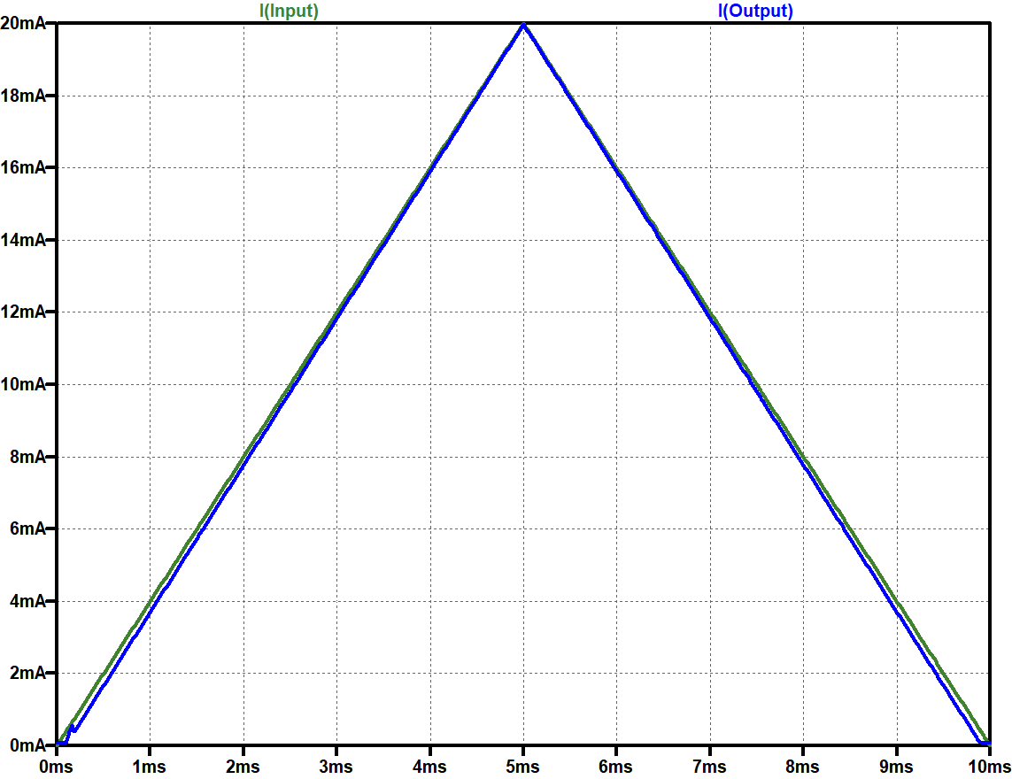
This circuit has been simulated in LTSpice using the available IL300 model from Vishay. The simulation is simply a transient simulation for a period of $10ms$. It sweeps the current from $0mA$ to $20mA$ then from $20mA$ to $0mA$. The coupling factors $K_1$ and $K_3$ are configurable using the parameters below $U_4$. After some minor tuning of the parameters to align for linearity and maximum output the following results have been achieved. Input Current is measured across the $I1$ current source, and $I(Output)$ is measured across $R_4$, or the isolated side resistor.
Additionally, we must perform a sanity check. Simulation models are not always correct under all conditions. We have to ensure that the current shunt is acting as we expect. For this we want to compare the current through the current shunt with the current through the LED. The target is to ensure that neither of these exceed $10mA$.
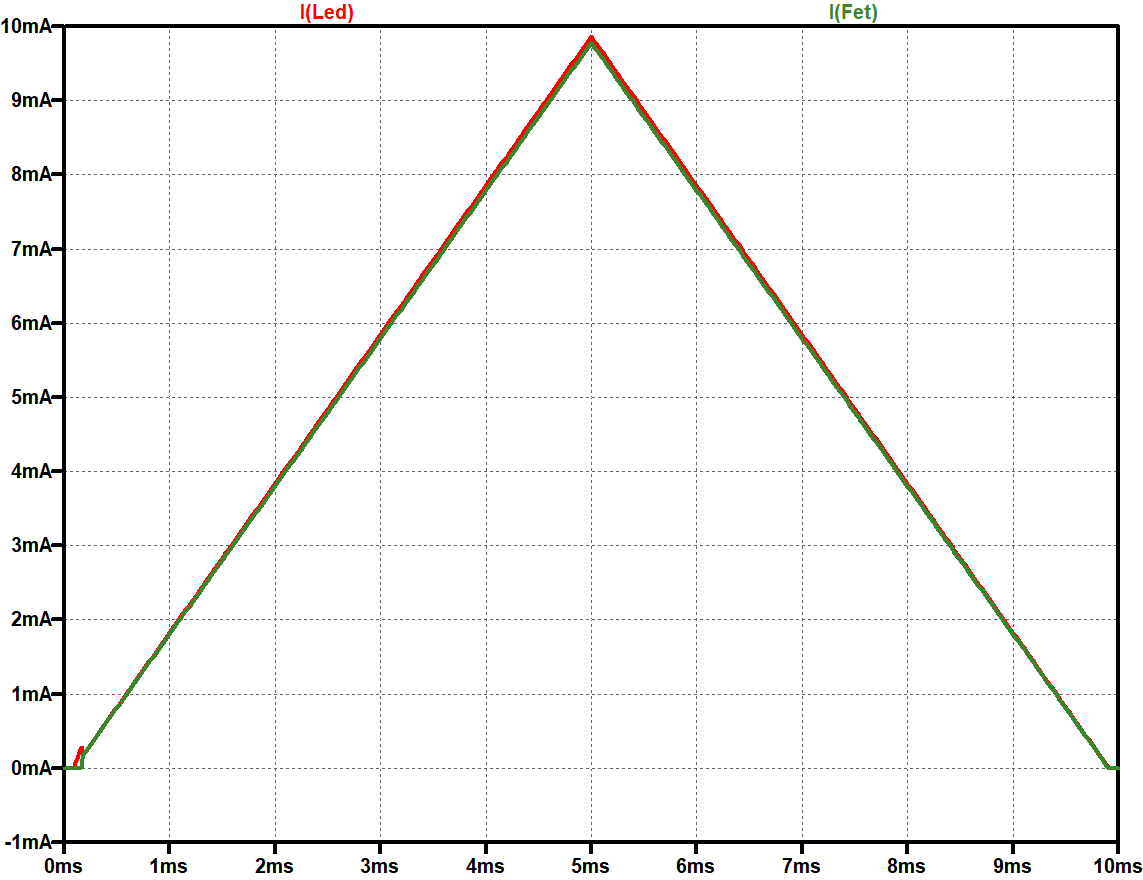
This confirms that the shunt is operating as expected. Once all the design requirements have been verified under nominal conditions it is then important to simulate, verify, and qualify that your product operates under all conditions including environmental effects, shock, vibration, and handling. A single SPICE simulation is insufficient to achieve all of these conditions.
Simulation Files
The simulation file can be downloaded here:
Other Applications
Linear isolators such as this can be used to isolate other signals such as voltage, or current which could be any analog signal. These circuits are used in isolation amplifiers as well as power supply feedback, especially in high voltage isolated systems to achieve isolation of voltage or current feedback signals.
Terms
| Term | Definition |
|---|---|
| Galvanic Isolation | The isolation of an electrical system to prevent the flow of current. |
| LED | Light Emitting Diode. |
| MOSFET | Metal Oxide Field Effect Transistor. |
| HART | Highway Addressable Remote Transducer Protocol. |
References
| Reference | Note |
|---|---|
| Vishay IL300 Datasheet | |
| Vishay AN54 - Isolated Industrial Current Loop Using the IL300 Linear Optocoupler | |
| Art of Electronics 3rd Edition Section 12.7.4 IV: Analog-oriented optocouplers | |
| Agilent Technologies - Optocoupler Designer’s Guide | |
| Avago AV02-4387EN - Optocouplers Designer’s Guide | Details reliability calculations. |
| Highway Addressable Remote Transducer Protocol (HART) | Protocol used with 4-20mA Loops. |
Table of Figures
- Isolated Receiver
- Voltage Loop Model
- Current Loop Model
- 4-20mA Current Loop, Modes of Operation
- Dual Photodiode (“Servo”) Optocoupler
- Simplified Design Overview
- Servo Gain vs Forward Current (IL300 Datasheet)
- Simulation Schematic
- Simulated Input vs Output Current
- Simulated FET vs LED Current